Problem: Distinguish between the terms “intrinsic semiconductor” and “extrinsic semiconductor“.
Solution: An intrinsic semiconductor is pretty much what it sounds like, i.e. a “pure” semiconductor material like \(\text{Si}\) that is undoped with any impurity dopants. An extrinsic semiconductor is then basically the negation of an intrinsic semiconductor, i.e. one which is doped with impurity dopants, although conceptually one can think of it as being doped with charge carriers (either holes \(h^+\) in a \(p\)-type extrinsic semiconductor or electrons \(e^-\) in an \(n\)-type extrinsic semiconductor).
Problem: In the phrases \(p\)-type semiconductor and \(n\)-type semiconductor, what do the \(p\) and \(n\) represent?
Solution: In both cases, the extrinsic semiconductor (isolated from anything else) is neutral, even when doped. Rather, the \(p\) and \(n\) refer to the majority mobile/free charge carriers in the corresponding semiconductor; i.e. holes in the valence band and electrons in the conduction band respectively.
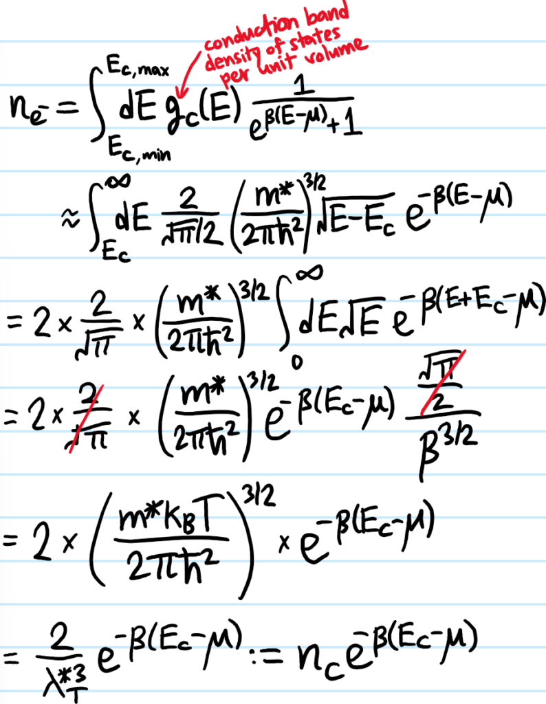
Problem: Show that the equilibrium number density \(n_{e^-}\) of mobile conduction electrons (i.e. not including the immobile core/valence electrons) thermally excited into the conduction band at temperature \(T\) is exponentially related to the gap \(E_C-\mu\) between the energy \(E_C\) at the base of the conduction band and the Fermi level \(\mu\):
\[n_{e^-}=n_Ce^{-\beta(E_C-\mu)}\]
where the so-called effective density of states:
\[n_C:=\frac{2g_v}{\lambda^{*3}_T}\]
is \(\approx\) the number density of available conduction band states at temperature \(T\) (here \(g_v\) is the valley degeneracy and \(\lambda^{*3}_T\) is the thermal de Broglie wavelength with respect to the electron’s effective mass \(m^*\)).
Solution: To clarify some of the approximations used in that line with the \(\approx\), the upper bound on the conduction band \(E_{C,\text{max}}\to\infty\) can be safely taken to infinity because of the exponential suppression of the integrand by the Fermi-Dirac distribution for \(E\gg\mu\) (in fact, using Fermi-Dirac statistics in the first place assumes the electrons interact solely through Pauli blocking). In addition, the density of states \(g_C(E)\) is approximated by that of a free particle in the neighbourhood of the conduction band valley (with the usual \(\sqrt{E}\mapsto \sqrt{E-E_C}\) because \(g_C(E)=0\) in the \(E\in[E_V,E_C]\) band gap) and with \(m\mapsto m^*\) to reflect the local curvature of the conduction band which is inherited from the strength of the lattice’s periodic potential. Finally, to strengthen the earlier claim that \(E\gg\mu\), indeed, \(E\geq E_C\) is the range of the integral, and so a sufficient condition for \(E\gg\mu\) is \(E_C\gg\mu\) (in practice a few \(k_BT\) is sufficient). This is assumed to be the case, and constitutes the assumption of a non-degenerate semiconductor (cf. non-degenerate Fermi gas). In this case, the Fermi-Dirac distribution boils down to just its “Boltzmann tail” \(\frac{1}{e^{\beta(E-\mu)}+1}\approx e^{-\beta(E-\mu)}\):
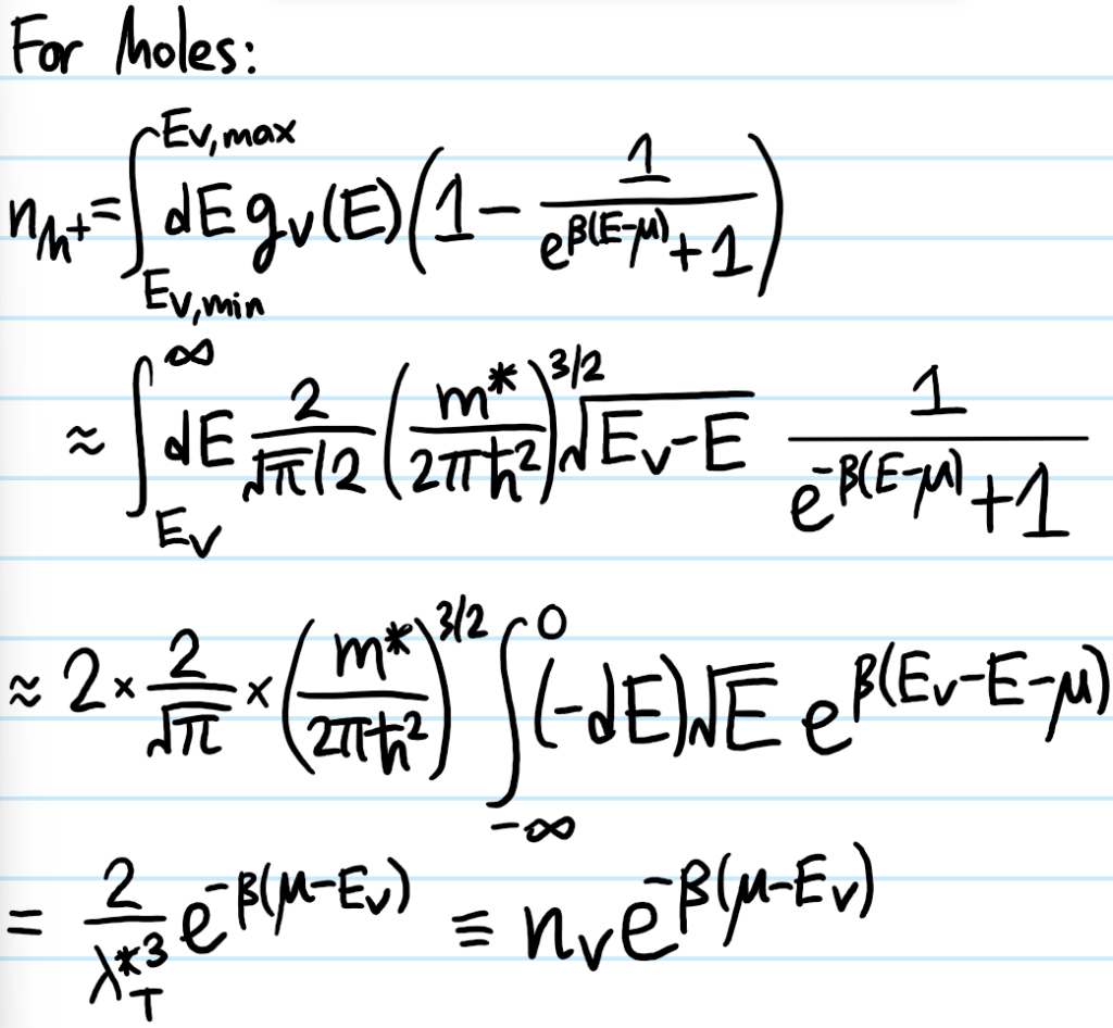
Problem: Repeat the above problem for holes to derive an analogous result for the equilibrium number density \(n_{h^+}\) of free conduction holes excited into the valence band at temperature \(T\):
\[n_{h^+}=n_Ve^{-\beta(\mu-E_V)}\]
where \(n_V\) is almost the same as \(n_C\) except that it’s derived from the effective mass \(m^*\) of the holes at the top of the valence band.
Solution: A few comments: if \(f(E)\) is the Fermi-Dirac distribution for electrons, then by the very definition of a hole as a vacancy/absence of an electron, the analog of the Fermi-Dirac distribution for holes (which can be considered fermionic quasiparticles) is \(1-f(E)\). In addition, a hole is considered to have more energy when it goes “downward” on a typical band diagram where the vertical axis \(E\) is really referring to the electron’s energy. This explains the counterintuitive limits on the integral:
Problem: If an intrinsic semiconductor is doped with impurity dopants to create an extrinsic semiconductor, say with a number density \(n_{d^+}\) of cationized donor dopants and \(n_{a^-}\) of anionized acceptor dopants, what constraint does charge neutrality of the semiconductor impose among the concentrations \(n_{e^-},n_{h^+},n_{d^+},n_{a^-}\)?
Solution:
\[-en_{e^-}+en_{h^+}+en_{d^+}-en_{a^-}=0\]
\[n_{h^+}+n_{d^+}=n_{e^-}+n_{a^-}\]
Conceptually, for every electron excited into the conduction band, the corresponding donor atom now becomes cationized; similarly, every hole excited into a valence band is really an acceptor atom anionizing as it accepts an electron from the valence band, so in the equation, it is conceptually meaningful to pair up \((n_{e^-},n_{d^+})\) and \((n_{h^+},n_{a^-})\). Note however this is not saying that they are equal; though they approach becoming equal the more heavily one dopes.
Problem: Show that, in an intrinsic semiconductor, the Fermi level \(\mu\) lies almost (but not exactly) at the midpoint \(\frac{E_V+E_C}{2}\) of the band gap.
Solution: An intrinsic semiconductor is undoped so \(n_{D^+}=n_{A^-}=0\). This implies from the charge neutrality argument above that \(n_{e^-}=n_{h^+}\) (i.e. every electron excited into the conduction band leaves a hole in the valence band). The rest of the argument is then just plugging in the earlier equilibrium free charge carrier concentrations and algebra:
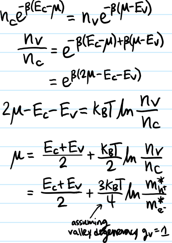
In what follows, it will be useful to call this particular value of \(\mu\) the intrinsic Fermi level \(\mu_i\) since it is the Fermi level of an intrinsic semiconductor, prior to any extrinsic doping.
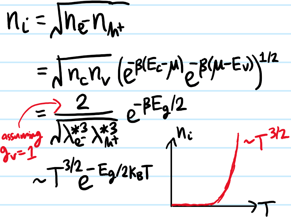
Problem: Define the intrinsic charge carrier concentration by \(n_i:=n_{e^-}=n_{h^+}\) for an intrinsic semiconductor, hence one has the so-called law of mass action \(n_{e^-}n_{h^+}=n_i^2\) (i.e. \(n_i^2\) is just a \(T\)-dependent equilibrium constant for the dissociation reaction \(0\to e^-+h^+\)). Show that the precise \(T\)-dependence of \(n_i\) is given by:
\[n_i\sim T^{3/2}e^{-E_g/2k_BT}\]
where the band gap \(E_g:=E_C-E_V\) (this result is sometimes also presented as \(n_i=n_Se^{-\beta E_g/2}\) where \(n_S:=\sqrt{n_Cn_V}\) is the geometric mean of the effective densities of states of the conduction and valence bands).
Solution:
Problem: Keeping tempertature \(T\) fixed, consider \(n\)-type doping an intrinsic semiconductor with donor dopants, thus creating an \(n\)-type extrinsic semiconductor. The effect of this will be to raise the Fermi level from the intrinsic Fermi level \(\mu_i\) (appx. in the middle of the band gap as shown earlier) to a new value \(\mu\) much closer to the base of the conduction band \(E_C\). Show that the precise amount of this raising can be quantified by:
\[\mu-\mu_i=k_BT\ln\frac{n_d}{n_i}\]
where \(n_d\) is the (directly manipulable!) concentration of donor dopants doped into the intrinsic semiconductor, stating the \(2\) key assumptions underlying this.
(note, an analogous line of reasoning for a \(p\)-type semiconductor shows that the Fermi level is lowered by an amount:
\[\mu_i-\mu=k_BT\ln\frac{n_a}{n_i}\]
where \(n_a\) is the (also directly manipulable) concentration of acceptor dopants).
Solution: At equilibrium, one has for an intrinsic semiconductor:
\[n_i=n_Ce^{-\beta(E_C-\mu_i)}\]
and for an \(n\)-type doped extrinsic semiconductor:
\[n_{e^-}=n_Ce^{-\beta(E_C-\mu)}\]
Taking the ratio yields:
\[\mu-\mu_i=k_BT\ln\frac{n_{e^-}}{n_i}\]
At this point, the goal is to justify why \(n_{e^-}\approx n_{d}\). This proceeds in \(2\) stages.
- First, justify that \(n_{e^-}\approx n_{d}^+\), the concentration of cationized donor dopants. This follows by setting \(n_{a^+}=0\) in the earlier charge neutrality constraint (since there are no acceptor dopants added \(n_a=0\Rightarrow n_{a^+}=0\)) and using the law of mass action to replace \(n_{h^+}=n_i^2/n_{e^-}\), obtaining a quadratic equation for \(n_{e^-}\) whose physical solution is:
\[n_{e^-}=\frac{n_{d^+}}{2}+\sqrt{\left(\frac{n_{d^+}}{2}\right)^2+n_i^2}\]
And at this point, one assumes that the semiconductor is fairly heavily doped, in particular \(n_D\gg n_i\) (typical values in \(\text{Si}\) are \(n_D\sim 10^{16}\text{ cm}^{-3}\) while \(n_i\sim 10^{10}\text{ cm}^{-3}\)). This allows one to approximate \(n_{e^-}\approx n_{d^+}\).
2. Then, to justify why \(n_{d^+}\approx n_d\), one has to assume that the donor dopants are shallow in the sense that the binding energy of their extra valence electron is comparable to \(k_BT\), and so it is easily excited into the conduction band. In other words, assume that almost complete cationization of donor dopants. This is just the statement that \(n_{d^+}\approx n_d\), as desired.
Problem: In what regime is the non-degenerate semiconductor approximation valid?
Solution: For an \(n\)-type extrinsic semiconductor, a rule of thumb is that the Fermi level cannot rise to within \(2k_BT\) of the base of the conduction band \(E_C\):
\[E_c-\mu\geq 2k_BT\]
Inserting \(n_d=n_Ce^{-\beta (E_C-\mu)}\) (where the approximation \(n_{e^-}\approx n_d\) has been employed), one arrives at the rule of thumb that the donor dopant concentration cannot exceed:
\[n_d\leq e^{-2}n_C\approx 0.14 n_C\]
Similarly, for \(p\)-type doping, the acceptor dopant concentration cannot exceed:
\[n_a\leq 0.14n_V\]
(the more important takeaway here is not the exact numerical prefactors, but the fact that the Fermi level should stay a few \(k_BT\) away from \(E_C\) or \(E_V\) for the semiconductor to be considered non-degenerate; indeed these estimates came from using the Boltzmann formula that was derived from this assumption, so it should be taken with a grain of salt as one is using a theory to predict its own demise).
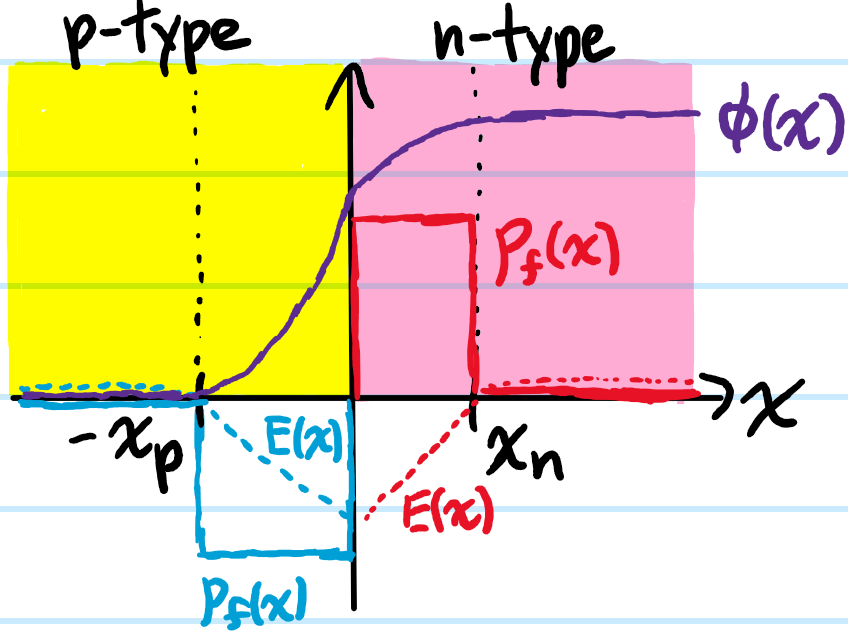
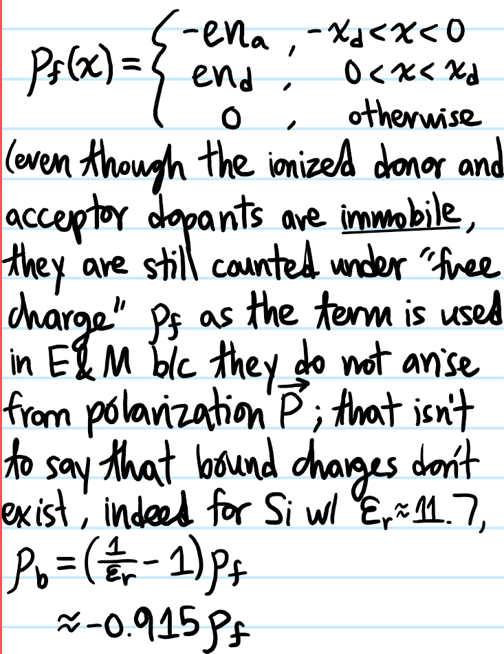
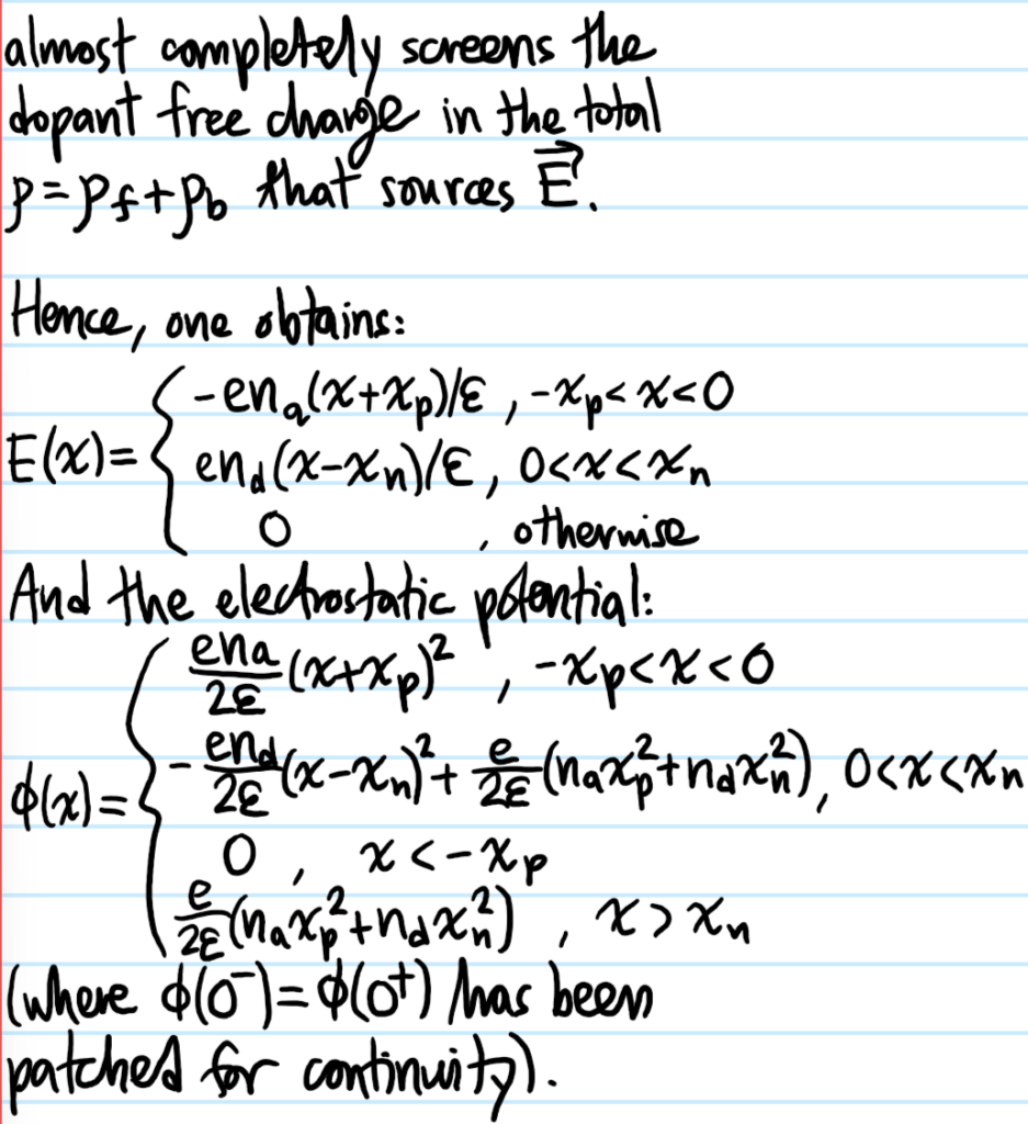
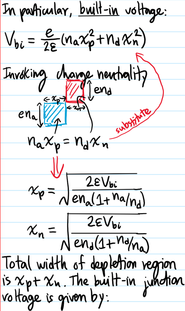
Problem: A \(p\)-\(n\) junction is formed by putting a \(p\)-type extrinsic semiconductor in contact with an \(n\)-type extrinsic semiconductor. Starting from a simple “top-hat” distribution of the free charge density \(\rho_f(x)\) in the depletion region \(-x_p<x<x_n\), sketch \(\rho_f(x)\), \(E(x)\) and \(\phi(x)\).
Solution: Assuming an abrupt junction and sharp cutoff for the depletion region at \(x_p, x_n\) respectively, one has:
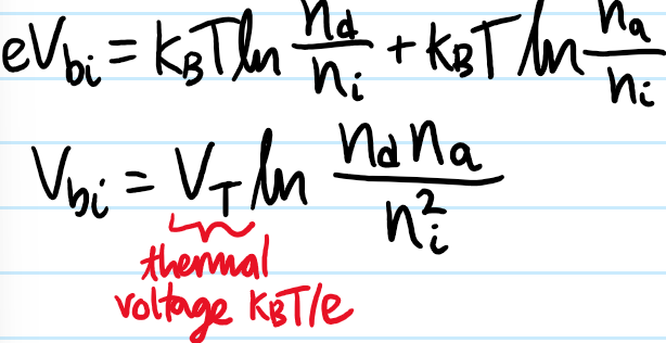
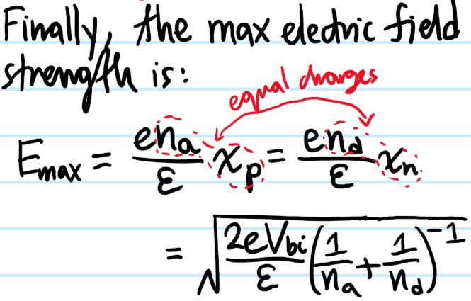
Problem: Make the sketches more quantitative. In particular, calculate the width \(x_n+x_p\) of the depletion region and the maximum strength \(E_{\text{max}}\) of the electrostatic field at the junction \(x=0\).
Solution:
Problem: Explain qualitatively how a depletion region forms at a \(p\)-\(n\) junction.
Solution: Intuitively, the electrons and holes cannot just keep diffusing indefinitely across the \(p\)-\(n\) junction because at some point too much like charge will clump on either side during recombination, preventing any further diffusion. Put another way, as the charge separation gets bigger and bigger, the induced \(\textbf E\)-field pointing from \(n\to p\) exerts an electric force on the electrons and holes that prevents them from crossing the junction; at equilibrium, this forms a depletion region where there are no mobile charge carriers.
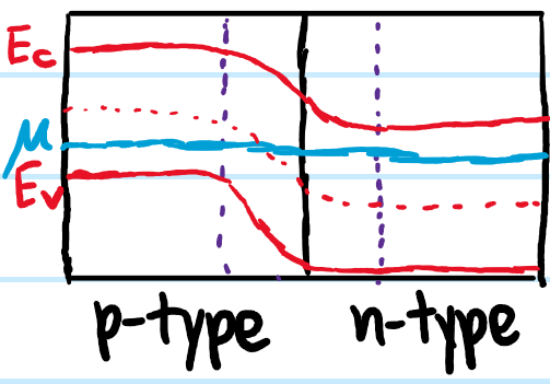
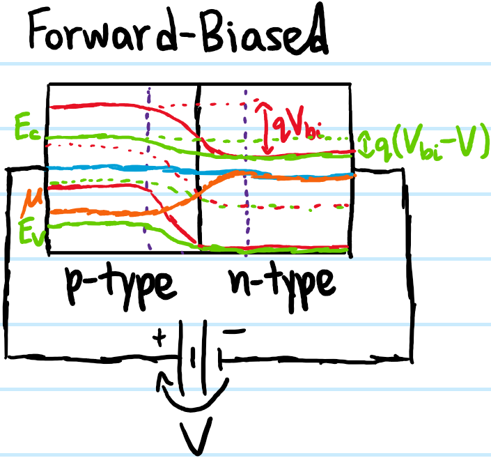
Problem: Just as a harmonic oscillator can be free or driven, so a \(p\)-\(n\) junction can also be “free” (just sitting there with its built-in potential \(V_{\text{bi}}\)) or it can be “driven” as well in a sense, more precisely by applying an external voltage \(V\) across it. However, unlike say with resistors/capacitors/inductors where the polarity of this voltage doesn’t really matter, here the asymmetry of the \(p\)-type vs. \(n\)-type semiconductors on either side, and thus the corresponding asymmetry of \(V_{\text{bi}}\), means that the polarity of \(V\) matters. Sketch qualitative band diagrams to show how the \(p\)-\(n\) junction’s bands change in the case of both forward bias \(V>0\) or reverse bias \(V<0\). This underlies the principle of operation for some (though not all) kinds of diodes, sometimes called a \(p\)-\(n\) semiconductor diode.
Solution: Some words of explanation: forward biasing a \(p\)-\(n\) junction lowers the effective built-in potential from \(V_{\text{bi}}\mapsto V_{\text{bi}}-V\). This clearly increases conductivity of both electrons and holes across the junction now that the energy barrier is reduced. By contrast, reverse biasing a \(p\)-\(n\) junction only raises the effective built-in potential \(V_{\text{bi}}\mapsto _{\text{bi}}+V\), reducing conductivity of electrons and holes as the depletion region gets bigger.
When the \(p\)-\(n\) junction is initially unbiased so that \(V=0\):
After forward biasing \(V>0\):
The reverse-biased case is just opposite to the forward-biased case, and not shown. Note also that this is not an instance of quantum tunnelling, because it’s not just a simple top-hat potential barrier, there is no probability current across the depletion region, and indeed also no electric current, only diffusion current as elaborated later.
Another way to put it is that forward-biasing the \(p\)-\(n\) junction encourages the majority charge carriers on each side to diffuse across the depletion region (and discourages the minority carriers, but that doesn’t matter anyways because they are minority), while reverse-bias is the opposite.
Problem: Recall that in an intrinsic semiconductor, at finite \(T>0\), the very few charge carriers in the conduction band are purely thermal electrons excited from their corresponding thermal holes in the valence band. Then, respectively \(p\)-type or \(n\)-type doping the intrinsic semiconductor, the creation of hydrogenic acceptor states just above the valence band or donor states just below the conduction band causes respectively holes to become the majority charge carrier (in the valence band) and electrons to become the minority charge carrier (in the conduction band) in the \(p\)-type extrinsic semiconductor, and vice versa for \(n\)-type (that isn’t to say that the thermal electrons and thermal holes \(n_{e^-,i}=n_{h^+,i}=n_i\sim 1.5\times 10^{10}\text{ cm}^{-3}\) aren’t still there, just they become negligible).
Solution:
Problem: Calculate the reverse saturation current \(I_{\text{sat}}=\lim_{V\to-\infty}I_{\text{sat}}(e^{V/V_T}-1)\) for a \(p\)-\(n\) junction semiconductor diode with the following parameters:
\[n_a=\]
Problem: Explain how a solar cell (aka photovoltaic cell) works.
Solution: Make a \(p\)-\(n\) junction out of either a direct bandgap (e.g. GaAs) or indirect bandgap (e.g. Si) semiconductor. Then, irradiate the depletion region of the \(p\)-\(n\) junction with photons of energy \(\hbar\omega\geq E_g\). This leads to \(\gamma\to e^-+h^+\) electron-hole pairs which get swept by the strong built-in \(\mathbf E\)-field according to \(\mathbf F=q\mathbf E\) with \(q=\pm e\). This can be used as a photocurrent to do work on a load. In practice, solar cells are made of multiple \(p\)-\(n\) junctions in order to surpass the Shockley-Queisser limit \(\eta\sim 1/3\) for a single \(p\)-\(n\) junction.
To sort out later:
At T=0 K, mu is not really well-defined (b/c g(E)=0 in the band gap, so mu could be put anywhere in there..) but for T>0 K it is well-defined…
For n-type doping, by putting extra atoms near the bottom of the conduction band, will increase the chemical potential…(all this comes from interpreting mu as a silly fit parameter that needs to be tuned to get integral g(E)f(E) = number density of conduction electrons in the system = number density of donor dopants).
For p-type doping, add strongly electronegative atoms, they rip off electrons from the valence band. leaving additional holes in the valence band.
w.r.t. intrinsic concentrations of electrons and holes at T=300 K,
something about asymmetry of the densities of states…the presence of the donor and acceptor states in the band gap influences g(E) there…